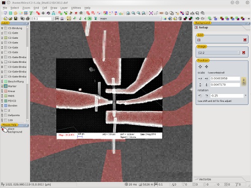
Nano-Tube Interconnection
Carbon nanotubes (CNTs) are allotropes of carbon with a cylindrical nanostructure. Nanotubes have been constructed with length-to-diameter ratio of up to 132,000,000:1,[1] significantly larger than any other material. These cylindrical carbon molecules have novel properties, making them potentially useful in many applications in nanotechnology, electronics, optics, and other fields of materials science, as well as potential uses in architectural fields. They may also have applications in the construction of body armor. They exhibit extraordinary strength and unique electrical properties, and are efficient thermal conductors. (from Wikipedia)
To use the unique electrical properties a electrical connection has to be created. This tutorial shows how to do that with the help of the LayoutEditor.
Step 1
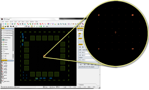
Pattern substrate with marker layout:
Step 2
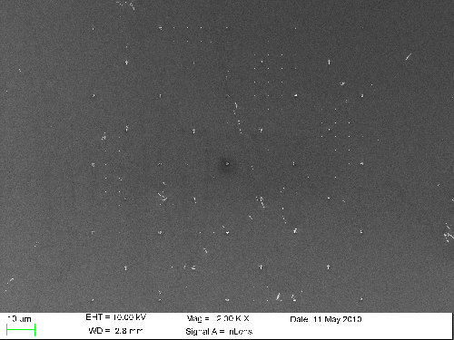
Fabricate nanotubes on substrate with alignment marks and take SEM image of fields:
Step 3
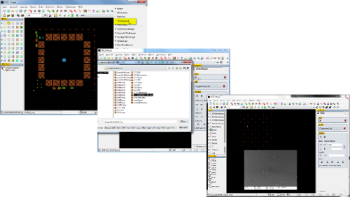
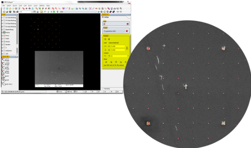
Open the LayoutEditor and load the SEM image as background:
Step 4
Use alignment function to bring marks of SEM image and the layout in alignment:
Step 5
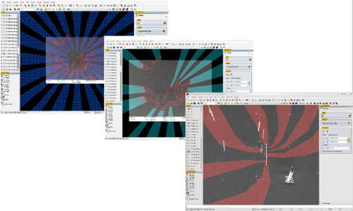
Draw layout according to nanotube position and interconnect with pads:
Step 6
Fabricate the design and check result:
